Chapter 24 — GPU Architecture for ML
“Understanding GPU architecture is understanding why certain operations are fast and others aren’t — the hardware shapes the software.”
Why GPUs for ML?
Deep learning is dominated by matrix multiplications, which are embarrassingly parallel. GPUs have thousands of cores designed for exactly this workload, while CPUs have a few complex cores designed for sequential tasks.
| Feature | CPU (AMD EPYC 9654) | GPU (NVIDIA H100 SXM) |
|---|---|---|
| Cores | 96 | 16,896 CUDA + 528 Tensor |
| Clock | 2.4 GHz | 1.6 GHz |
| FP16 TFLOPS | ~1 | 1,979 (Tensor Core) |
| Memory | 768 GB DDR5 | 80 GB HBM3 |
| Bandwidth | 460 GB/s | 3,350 GB/s |
| TDP | 360W | 700W |
NVIDIA GPU Anatomy
Streaming Multiprocessor (SM)
The SM is where computation happens. Each SM (H100) contains:
- 128 FP32 CUDA cores — general-purpose floating-point
- 4 Tensor Cores — specialized 4×4 matrix multiply-accumulate units
- 256 KB register file — fastest storage
- 256 KB configurable shared memory / L1 cache
- Warp schedulers that manage 32-thread groups
Memory Hierarchy
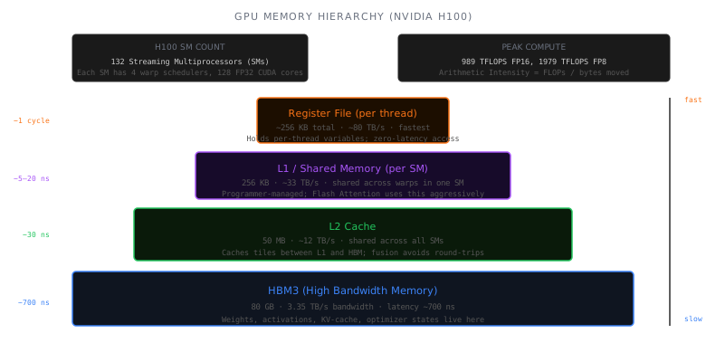
The critical insight: there’s a 1000× gap between SRAM speed (~20 TB/s) and HBM speed (~3.35 TB/s). This is why kernel fusion (combining operations to keep data in SRAM) and tiling (processing data in cache-friendly blocks) are so important.
Compute-Bound vs Memory-Bound
The roofline model determines whether an operation is limited by compute speed or memory bandwidth:
Arithmetic Intensity = FLOPs / Bytes transferred
- Arithmetic intensity > machine's ratio
- Large matrix multiplications (training, prefill)
- Solution: more FLOPS (bigger GPU, Tensor Cores)
- Example: [4096, 4096] × [4096, 4096]
- Arithmetic intensity < machine's ratio
- Decode step (read model + KV-cache for 1 token)
- Solution: more bandwidth (quantization, HBM3e)
- Example: element-wise ops, attention decode
For H100: peak compute is ~1979 TFLOPS FP16, bandwidth is 3350 GB/s. The balance point is ~590 FLOPs per byte. Operations below this ratio are memory-bound.
LLM inference decode is almost always memory-bound — you read the entire model from HBM for each token, but only do one matrix-vector multiply per layer.
FLOPS Calculation for Matrix Multiply
For $C = A \times B$ where $A: [M, K]$, $B: [K, N]$:
\[\text{FLOPs} = 2 \times M \times N \times K\](Each element of C requires K multiplications + K-1 additions ≈ 2K FLOPs.)
| Operation | M | K | N | FLOPs | Time at 1000 TFLOPS |
|---|---|---|---|---|---|
| QKV projection | 4096 | 4096 | 3×4096 | 103 GFLOP | 0.1 ms |
| FFN (SwiGLU forward) | 4096 | 4096 | 3×14336 | 724 GFLOP | 0.7 ms |
| Decode (batch=1) | 1 | 4096 | 4096 | 33 MFLOP | 0.00003 ms |
The decode QKV projection does 33 MFLOP but reads ~34 MB of weights — completely memory-bound.
Key GPU Comparison
| GPU | Architecture | HBM | Bandwidth | FP16 TFLOPS | Tensor Core | PCIe/NVLink |
|---|---|---|---|---|---|---|
| RTX 4090 | Ada Lovelace | 24 GB GDDR6X | 1,008 GB/s | 330 | 4th gen | PCIe 4.0 |
| A100 80GB | Ampere | 80 GB HBM2e | 2,039 GB/s | 312 | 3rd gen | NVLink 600 GB/s |
| H100 SXM | Hopper | 80 GB HBM3 | 3,350 GB/s | 1,979 | 4th gen + FP8 | NVLink 900 GB/s |
| H200 | Hopper | 141 GB HBM3e | 4,800 GB/s | 1,979 | 4th gen + FP8 | NVLink 900 GB/s |
| B200 | Blackwell | 192 GB HBM3e | 8,000 GB/s | 4,500 | 5th gen + FP4 | NVLink 1800 GB/s |
The evolution trend: HBM capacity and bandwidth are growing faster than compute TFLOPS, reflecting the memory-bound nature of LLM inference.
Tensor Cores
Tensor Cores are specialized units that perform matrix multiply-accumulate on small matrices (4×4, 8×8, or 16×16) in a single clock cycle. They are dramatically faster than CUDA cores for matrix operations:
| Operation | CUDA Cores | Tensor Cores | Speedup |
|---|---|---|---|
| FP16 matmul | 312 TFLOPS | 1,979 TFLOPS | 6.3× |
| FP8 matmul | — | 3,958 TFLOPS | 12.7× |
| INT8 matmul | — | 3,958 TOPS | 12.7× |
Tensor Cores require specific matrix dimension alignment (multiples of 8 or 16) for maximum efficiency. This is why model dimensions are typically multiples of 128.
What’s Next
Understanding GPU architecture motivates CUDA and kernel development — writing custom operations that exploit the memory hierarchy for maximum performance.
← Previous: Chapter 23 — Knowledge Distillation & QAD · Next: Chapter 25 — CUDA & Kernel Development →
Last updated: April 2026